Joint Design Manufacturing (JDM) for Software-First, AI-Driven Teams
JDM — Joint Design Manufacturing built exclusively for software-first and AI-driven teams. You maintain absolute control over the application layer and product roadmap. We operate as your dedicated hardware department—delivering custom PCBA architecture, hardware bring-up, and robust BSPs. Get a deployment-ready hardware platform designed for volume production, without the overhead of an in-house hardware team.
When You Have the Software Stack — But Need the Hardware Execution
Joint Design Manufacturing (JDM) bridges the gap between software-first / AI-driven companies and the physical manufacturing resources they lack. If you own the algorithms, the application stack, and a target market—but lack an in-house embedded hardware team—JDM gives you a dedicated, turnkey PCBA engineering department without the overhead.
JDM is a deeply transparent, co-engineering model. You drive the application logic and system architecture, while our engineers work as a seamless extension of your team. We deliver high-speed schematics, PCBA layouts, and production-ready manufacturing under a shared agile roadmap. By handling the heavy lifting of custom board bring-up, BSP development, and low-level firmware integration, we deliver a stable, deployment-ready hardware platform so your team can focus entirely on what you do best: building and scaling your software.
Your application code, AI models, or OS-level software are solid, but custom PCBA design and bare-metal firmware/BSP development are blind spots. We bridge the gap.
You know exactly what the hardware needs to execute (Block Diagrams / System Specs). We translate your vision into production-ready schematics and high-yield, production-grade PCBA layouts.
You want a true technical partner, not a black-box factory. You get direct, weekly access to our senior hardware architects to participate in design reviews and BOM selections—no middlemen.
Our Build-to-Print OEM/EMS model is faster and more cost-efficient for you.
JDM is built for teams that already own the core software stack. If you have a market need and a Product Requirements Document (PRD), and need a partner to develop the entire custom solution from scratch—both hardware and firmware—explore our Turnkey ODM is your best path.
Full PCBA Engineering Stack
As a JDM partner, you unlock the complete hardware infrastructure that powers our Turnkey ODM—while your team maintains absolute control over the system architecture.
PCBA Design & Engineering
Co-develop system block diagrams, SoC selection, high-speed HDI layout, and embedded firmware & BSP. Thermal management strategies and rigorous DFM/DFT reviews are mandatory before any board release.
Explore Design & Engineering →Prototyping & Manufacturing
Leverage in-house quick-turn PCBA prototyping, seamlessly scaling to volume production on 4× Yamaha YSM20 SMT lines equipped with inline 3D SPI, AOI, and X-Ray inspection.
Explore Manufacturing & Assembly →Testing & Pre-Compliance
Custom ICT/FCT test fixture engineering, environmental stress screening, and EMC pre-compliance scanning—eliminating hardware risks long before market deployment.
Explore Testing & Compliance →Co-Development: Your Team + Our Engineers
A collaborative turnkey PCBA workflow where your software or AI team drives the application logic — and our engineers handle the physical execution. Delivered in transparent phases from architecture to volume production.
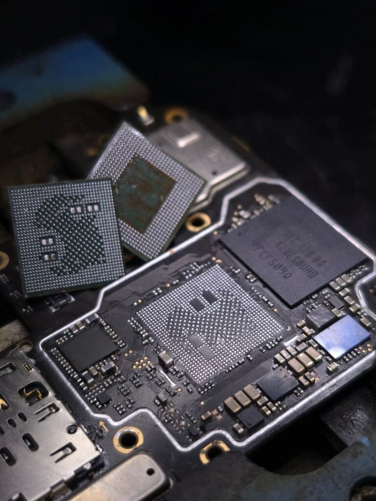
Joint Architecture & SoC Selection
Together with your software and AI team, we translate your product spec into a robust hardware architecture. We present 2-3 SoC/MPU options detailing cost vs. performance trade-offs — your team makes the final call. Your software stack preferences (Linux, RTOS, bare-metal, edge inference framework) shape every hardware decision from day one.
Collaborative Schematic & PCB Layout
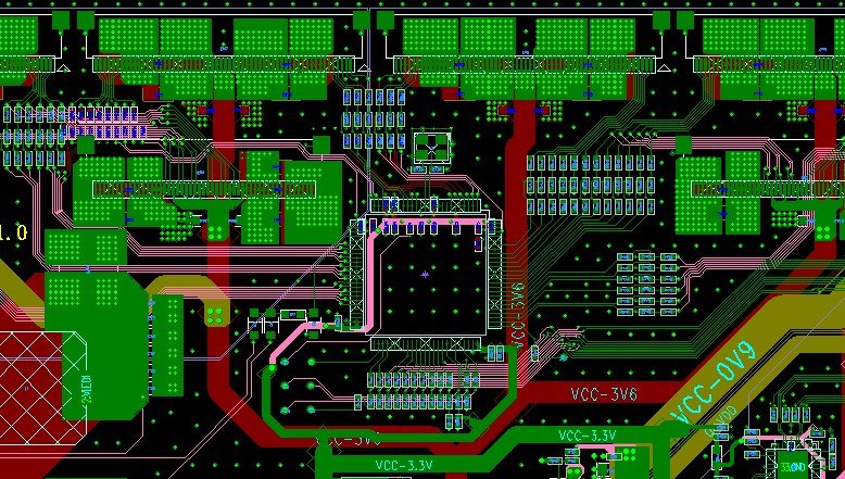
No layout proceeds without your schematic sign-off. We execute schematic capture with full DRC, and high-speed HDI PCB routing backed by strict impedance control and thermal management strategies. Every design undergoes rigorous DFM and DFT reviews before release — eliminating costly re-spins before your team sees a single prototype.
 LAYOUT
 Prototyping & Joint Validation (EVT/DVT)
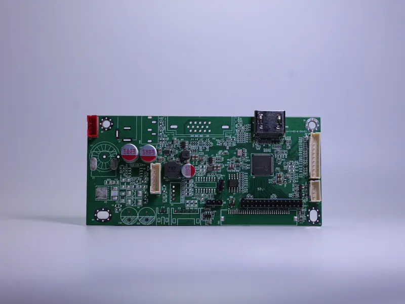
We provide BSP, low-level firmware, and OS integration — your application team deploys on top. In-house quick-turn PCBA prototyping delivers EVT boards loaded with a full board support package. We handle environmental stress testing and iterative DVT cycles; your team focuses purely on application-layer code and AI model deployment while we validate the physical hardware.
 PROTOTYPE
 NPI, Compliance & Production Ramp
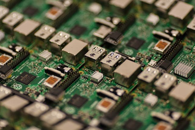
Design validated. Production ready — on our SMT lines. We develop custom FCT/ICT fixtures, complete CE/FCC pre-compliance scanning, and execute the strict NPI transition. The complete technical IP is managed or transferred based on your selected transparent NRE model (Full IP Handoff vs. Volume Partnership) — though most clients continue manufacturing with us for continuity, traceability, and an engineering team that knows their board best.
 PRODUCTION
How We Collaborate: Engineering as One Team
Transparency is the foundation of every Joint Design Manufacturing (JDM) engagement. We don't just build your hardware; we integrate seamlessly into your engineering workflow. Here is what the day-to-day partnership looks like.
Communication Rhythm & Agile Sync
JDM is built around direct collaboration between your technical lead and a dedicated senior hardware architect on our side. We adapt to your team's rhythm—whether that means syncing via Slack/Teams or tracking issues in Jira. Alignment on system architecture, schematic capture, HDI layout review, and EVT acceptance aren't just emails; they are formal, documented milestones with mandatory sign-offs at each gate.
NDA & Intellectual Property
Every engagement begins with a mutual NDA signed before the first technical discussion — this is the industry prerequisite that protects both sides' engineering integrity from day one, not a negotiation point.
When it comes to Intellectual Property (IP) and design files, we believe in giving you the choice. We offer two transparent commercial paths to balance your upfront budget and long-term IP ownership needs:
- Full IP Handoff (Standard NRE + Volume Deposit) — You pay the standard NRE fee plus a separate, refundable manufacturing deposit upfront. Once your cumulative production volume reaches the agreed target, 100% of the native design files are permanently unlocked and transferred to your team. The deposit is then fully refunded.
- Volume Partnership (Subsidized R&D) — We heavily subsidize the upfront NRE cost to lower your initial barrier. In exchange, JUZHITECH retains the design files and acts as your exclusive, long-term Turnkey manufacturing partner.
"In our JDM model, you talk directly to the engineer routing your board—not a sales rep. Your technical lead holds veto power at every major design gate. We bring the embedded hardware department you don’t have in-house, with absolute transparency."
Engineering Decision Points You Control
We do the heavy lifting, but you hold the steering wheel. We consult; you decide.
- SoC / MPU Architecture Selection — We present 2-3 chipset options detailing trade-offs in cost, supply chain availability, and software ecosystem support. You make the final call.
- BOM Cost vs. Performance Trade-offs — We engineer both cost-optimized and performance-optimized BOM variants (e.g., memory sizing, power management ICs). You decide the balance.
- Mandatory Design Review Gates — No PCB layout proceeds without your schematic sign-off. No physical prototypes are fabricated without your layout approval.
- Global Certification Strategy — We recommend the regulatory pathways (CE, FCC, UL) relevant to your target deployment. You select which markets to pursue and at what prototyping stage.
What We Need From You
- System Architecture & Block Diagrams — You provide the high-level system logic, target performance, interfaces, and form factor constraints.
- A Designated Technical Point of Contact — For ongoing design reviews, Jira ticket resolutions, and milestone sign-offs.
- Access to Your Application/Software Team — We handle the custom board bring-up, BSP, and OS integration; your team deploys and tests the application layer.
- Target BOM Cost & Volume Projections — To guide our component sourcing strategy and lifecycle management during the design phase.
JDM Deliverables — The "App-Ready" Hardware Package
At the end of a JDM engagement, you receive fully validated, mass-production-ready PCBA hardware alongside the complete source files and custom BSP — not just raw prototypes.
Native schematics, high-speed PCB layouts (Gerbers / ODB++), and validated BOMs. Full source files and 100% IP ownership are transferred according to your selected NRE engagement model (Volume Partnership vs. Full IP Handoff).
Fully assembled, functionally tested PCBA batches (EVT/DVT). Delivered pre-flashed with your custom Board Support Package (BSP), low-level drivers, and bootloader—ready for your app deployment.
Impedance control reports, thermal profiling data, environmental stress test results (temperature cycling, humidity, vibration), and EMC pre-compliance scan reports.
Manufacturing SOPs, custom ICT/FCT test fixture designs, acceptance criteria, and a seamless transition plan for volume SMT production — whether you scale at our facility or yours.
Not the Right Model for You?
Side-by-Side Model Matrix
Compare OEM/EMS, JDM, and ODM models across critical dimensions — from required engineering inputs and IP ownership (NRE structures) to final PCBA deliverables.
View Matrix →Turnkey ODM Development
Starting from a PRD or market concept. We take full lifecycle ownership of the hardware architecture, OS-level firmware, CE/FCC certification, and final box-build delivery.
Explore Turnkey ODM →Build-to-Print OEM/EMS
Your completed Gerber files and BOM, our manufacturing precision. We execute rigorous DFM reviews, turnkey component sourcing, and high-yield SMT assembly.
Explore OEM / EMS →common questions
Common Questions About JDM
We're a software/AI company — what hardware input do you need from us?
Very little — that’s the point of JDM. Bring us your target specs (performance, interfaces, form factor), your software stack preferences (Linux, RTOS, bare-metal), and your system block diagrams or API definitions. We handle everything hardware-related: SoC selection, schematic capture, PCB layout, prototyping, and manufacturing. If you’re not sure about certain specs yet, our architects will help you define what’s realistic at your target BOM cost.
What's the typical JDM timeline from concept to production?
Timelines scale with architectural complexity. A single-MCU IoT controller moves significantly faster than a multi-processor HDI edge computing board. The JDM advantage is parallel development: while we route the high-speed PCB, your team receives early BSP drops and dev boards to begin software porting immediately. A detailed, agile milestone schedule is locked in during the initial proposal.
Can you also advise on enclosure design and product-level decisions?
Yes. While JDM’s core is custom PCBA and BSP delivery, our engineering team has deep expertise in electromechanical integration. We advise on thermal dissipation structures, connector placement, and custom test fixtures. If you require a complete “Box-Build” solution, we can seamlessly integrate the engineered board into your industrial enclosure on our assembly lines.
How exactly does JDM differ from Turnkey ODM?
The difference lies in where your team’s engineering stops and ours begins.
In JDM, you bring an active software/AI team. You write the application code; we design the hardware and provide the low-level BSP/drivers to bridge the gap. It is a highly collaborative, side-by-side co-engineering model.
In ODM, you are starting with a market concept or a Product Requirements Document (PRD). We act as your entire turnkey engineering department, managing everything from bare-metal firmware to hardware layout, delivering a ready-to-deploy hardware solution.
Can your hardware engineers work directly with our software team?
Absolutely—that is the defining feature of JDM. We bypass the “sales rep” bottleneck. Your CTO or lead developer syncs directly with our senior hardware architects. We establish clear boundaries at the Hardware Abstraction Layer (HAL): we provide the BSP, bootloader, and bring-up support; your team deploys the application layer on top.
How do you protect our proprietary software and algorithms?
IP protection is non-negotiable. We operate under strict mutual NDAs signed before the first technical discussion. Furthermore, in a JDM engagement, your application logic and AI models remain strictly yours—they are often flashed post-production or encrypted. For the hardware design IP (schematics, PCB layout), we offer clearly defined, transparent NRE structures: either subsidized Volume Partnerships or Full IP Handoff upon reaching production targets, ensuring your technical assets are secured according to your long-term strategy.
Three Steps from Requirements to Kickoff
Every JDM engagement starts with an engineer-to-engineer sync — no friction, zero obligation.
Share Your Product Spec
Send us your system block diagram, target performance metrics, or software stack requirements. We adapt to your workflow — no rigid formats required.
Architecture Feasibility Call
A senior hardware architect reviews your specs and schedules a 60-minute technical alignment call. NDA signed. Feedback within 48 hours.
NRE Proposal & Kickoff
Receive a detailed blueprint: custom PCBA architecture, BSP development scope, target BOM cost, and flexible NRE options. You approve, we start engineering.
All submissions protected under NDA by default.