Our PCBA Manufacturing Capabilities
JUZHITECH's one-stop PCBA services are powered by our state-of-the-art 11,000 m² facility. With 7 SMT lines, 300K joints/hour output, and a 48-hour quick-turn capability, we turn your designs into IPC-A-610 Class 2/3 quality products.
Total Facility Area
PCB fabrication + SMT assembly under one quality system — up to 32 PCB layers, from bare board to tested PCBA.
SMT Lines · 5 MP + 2 NPI
Solder Joints / Hour
Quick-Turn · >95% on-time
PCB Output / Month
In-House Manufacturing
Walk the Floor — Virtually
11,000 m² across a PCB fabrication plant and an SMT assembly plant — one quality system, no vendor handoff. Click any image to enlarge.
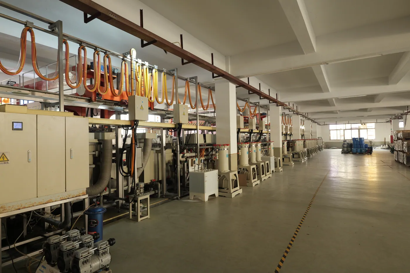 PCB Fabrication Plant
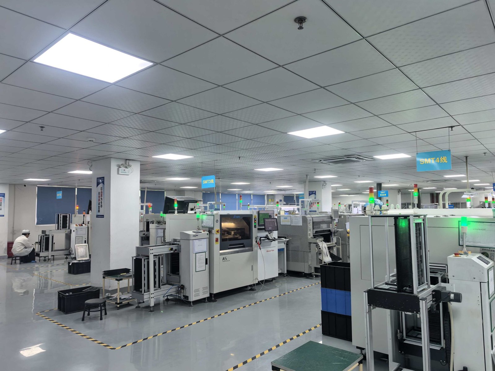 SMT Assembly Plant
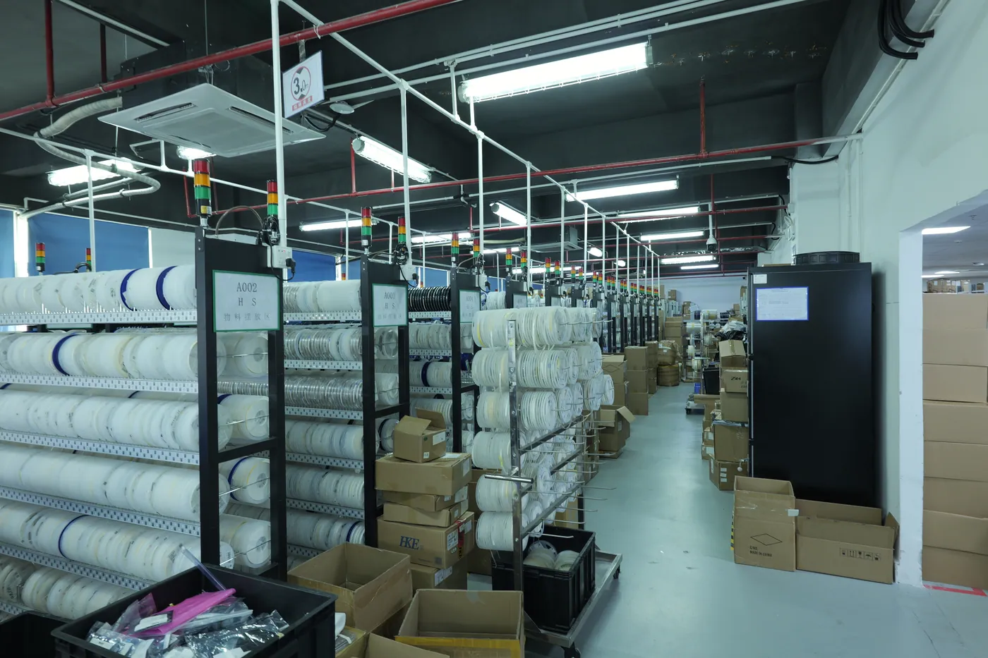 Component Warehouse
PCB Fabrication
Bare-Board Plant
We fabricate our own bare boards — so stackup, impedance, and copper are controlled in-house from day one.
- 12,000 m²/month output capacity
- Up to 32 layers · 2.5/2.5 mil line/space (HDI)
- ±5% differential impedance (TDR + back-drilling)
- 1st-order laser via + back-drilling
- ENIG · immersion silver · OSP · LF-HASL · hard gold
SMT Assembly
Assembly & Test Plant
A 48-hour quick-turn SMT plant for prototype, pilot, and low-to-mid volume — with test and finishing under the same roof.
- 7 SMT lines (5 mass production + 2 NPI)
- 300,000 joints/hour capacity
- 48h quick-turn, >95% on-time
- 03015 chip / 0.35mm-pitch BGA (IC ±0.025mm)
- 4 test lines + 1 assembly line (FCT · aging · temp/humidity · vibration)
Production Flow
One Continuous Line, Thirteen Stages
A board moves through thirteen stages without leaving the floor — fewer handoffs, fewer mistakes, tighter traceability.
◉ Terminus — Bare boards from our in-house PCB fab
Incoming & IQC
Barcode receiving, bridge-tested passives, first-article tester before anything is loaded.
Stencil Printing
Automatic solder-paste printing with 3D SPI verification on every deposit.
SMT Pick & Place
High-speed placement across all lines — 03015 chips to 45mm packages at 0.35mm pitch.
First-Article (FAI)
3–5 pc trial run; engineering, production, quality & test sign-off before batch.
Reflow
Reflow soldering per J-STD-020 profile, verified on first article for every work order.
Inline AOI
100% post-reflow 3D inspection — solder joints, polarity, presence.
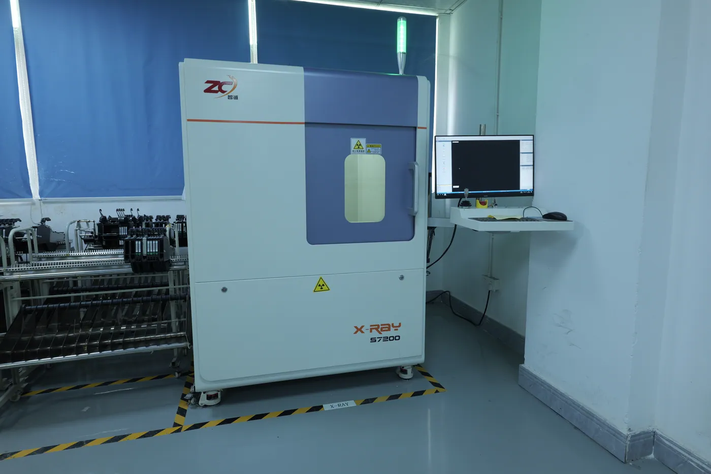
X-Ray
Every BGA/QFN hidden joint — voids checked against IPC-7095.
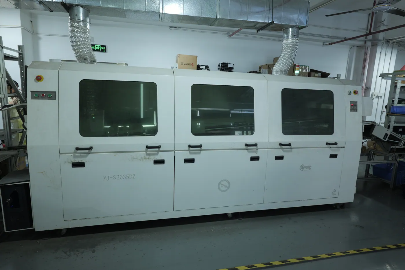
DIP & Wave
Through-hole insertion, wave + selective soldering, hand-solder stations.
ICT / FCT
Bed-of-nails + functional test — boot sequence, I/O, and RF performance.
Aging & Stress
Burn-in, temperature/humidity cycling, vibration per your spec.
Conformal Coating
UV-cure conformal coating, fluorescent coverage verification.
Final QC (OQC)
Outgoing audit on every batch before packing — see the quality gates below.
Packing & Ship
ESD-safe packaging, drop-ship ready, per-serial traceability file.
◉ Terminus — Tested PCBA · ESD-packed · Shipped
Core Equipment
The Line, Part by Part
The equipment behind the numbers — both fabrication and assembly. Every unit runs on a maintenance and calibration schedule.
PCB Fabrication
Bare-board plant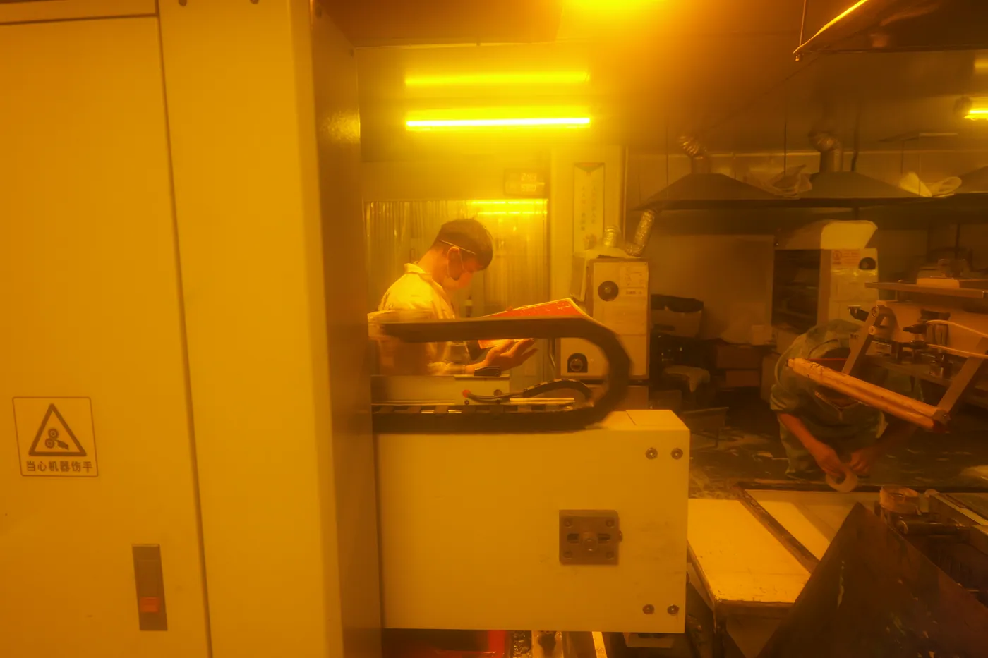
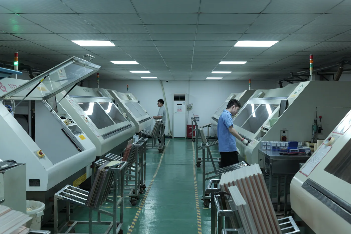
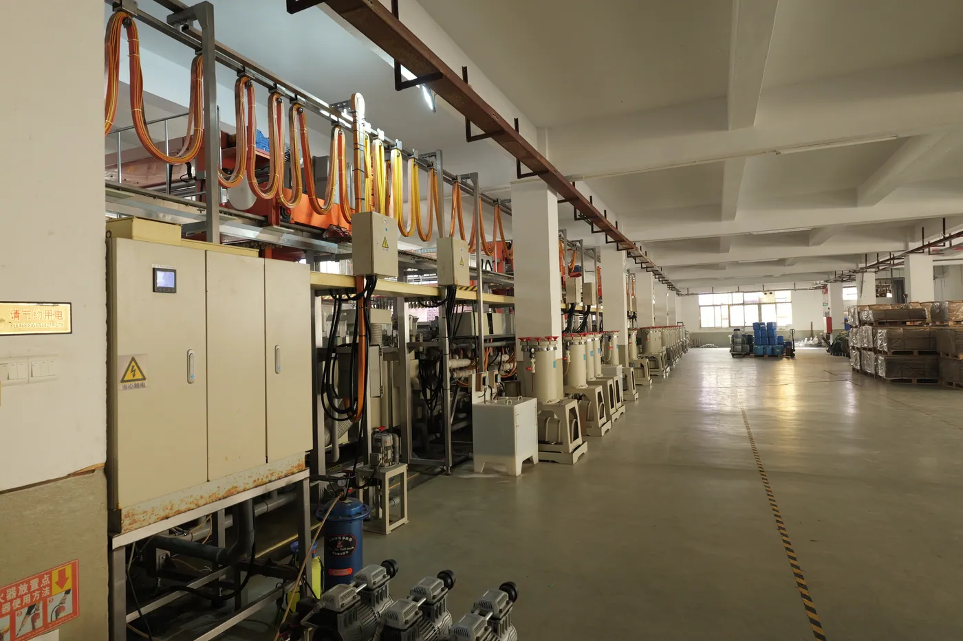
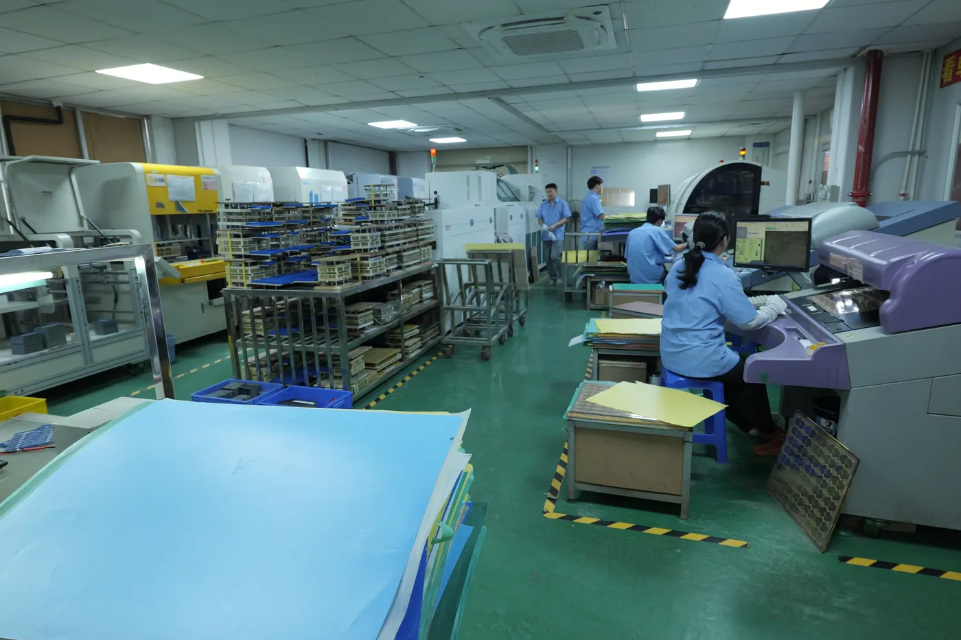
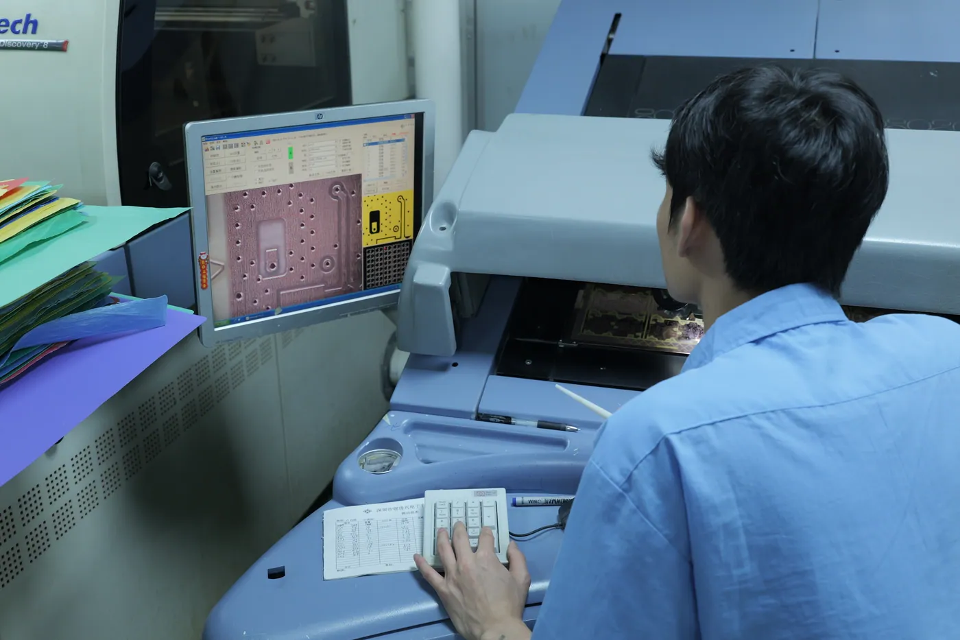
LDI imaging
Fine traces · 2.5 mil HDI
6-axis drilling
Min hole 0.15 mm
Plating / etch / PTH
Multilayer build-up
Probe + E-test + AOI
Electrical verification
Back-drill + scope
Impedance & via check
SMT Assembly
Assembly & test plant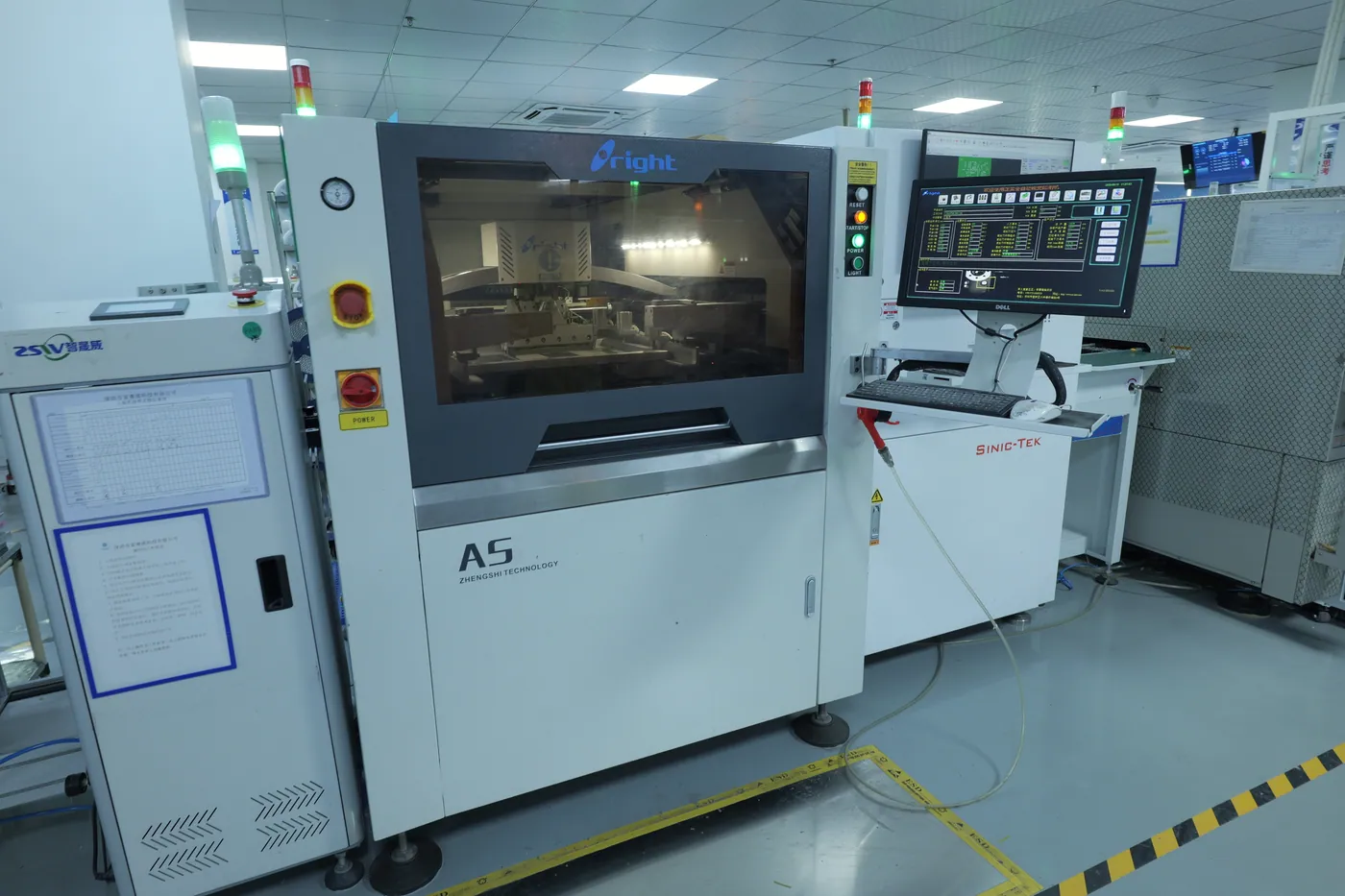
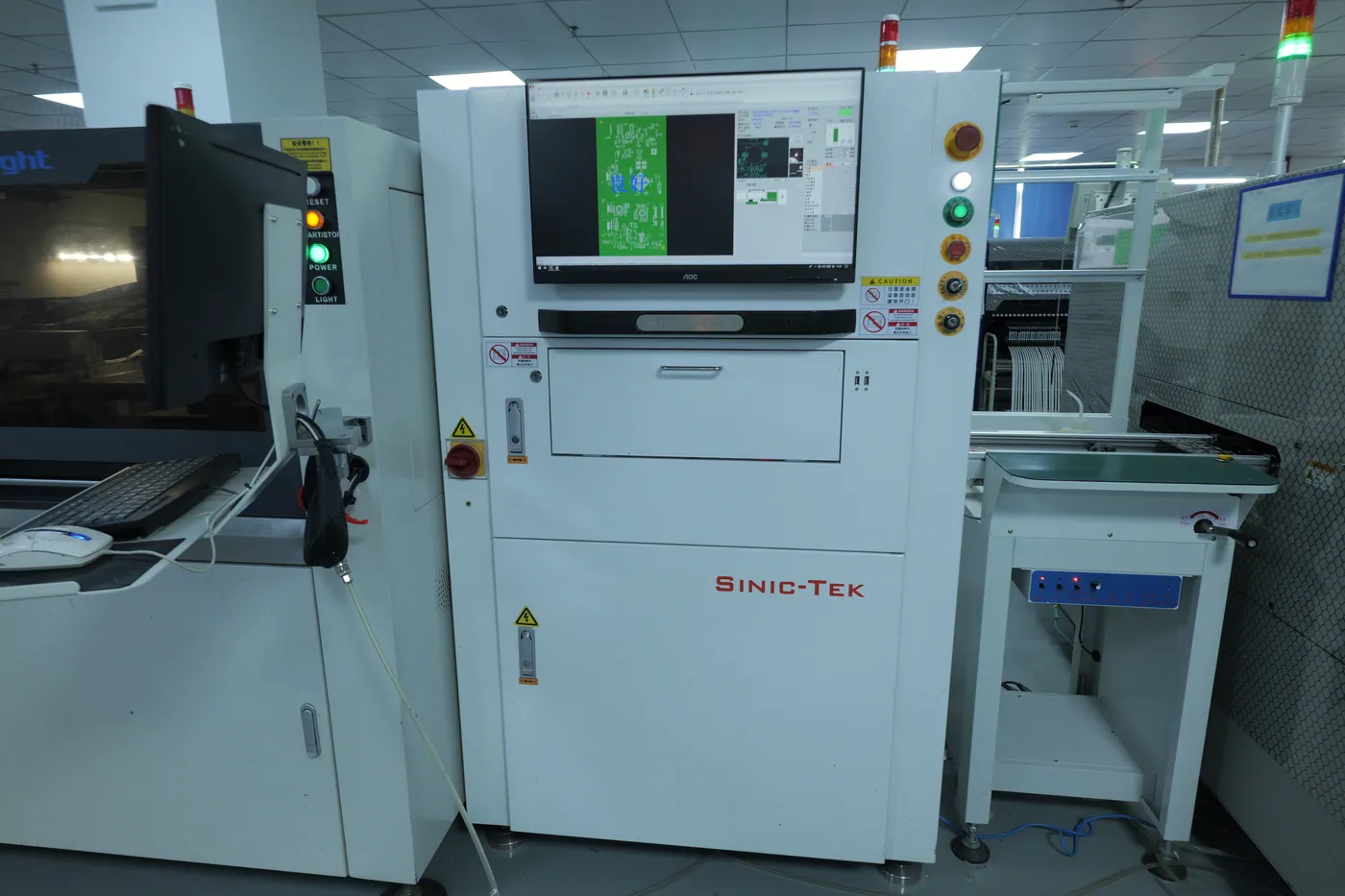
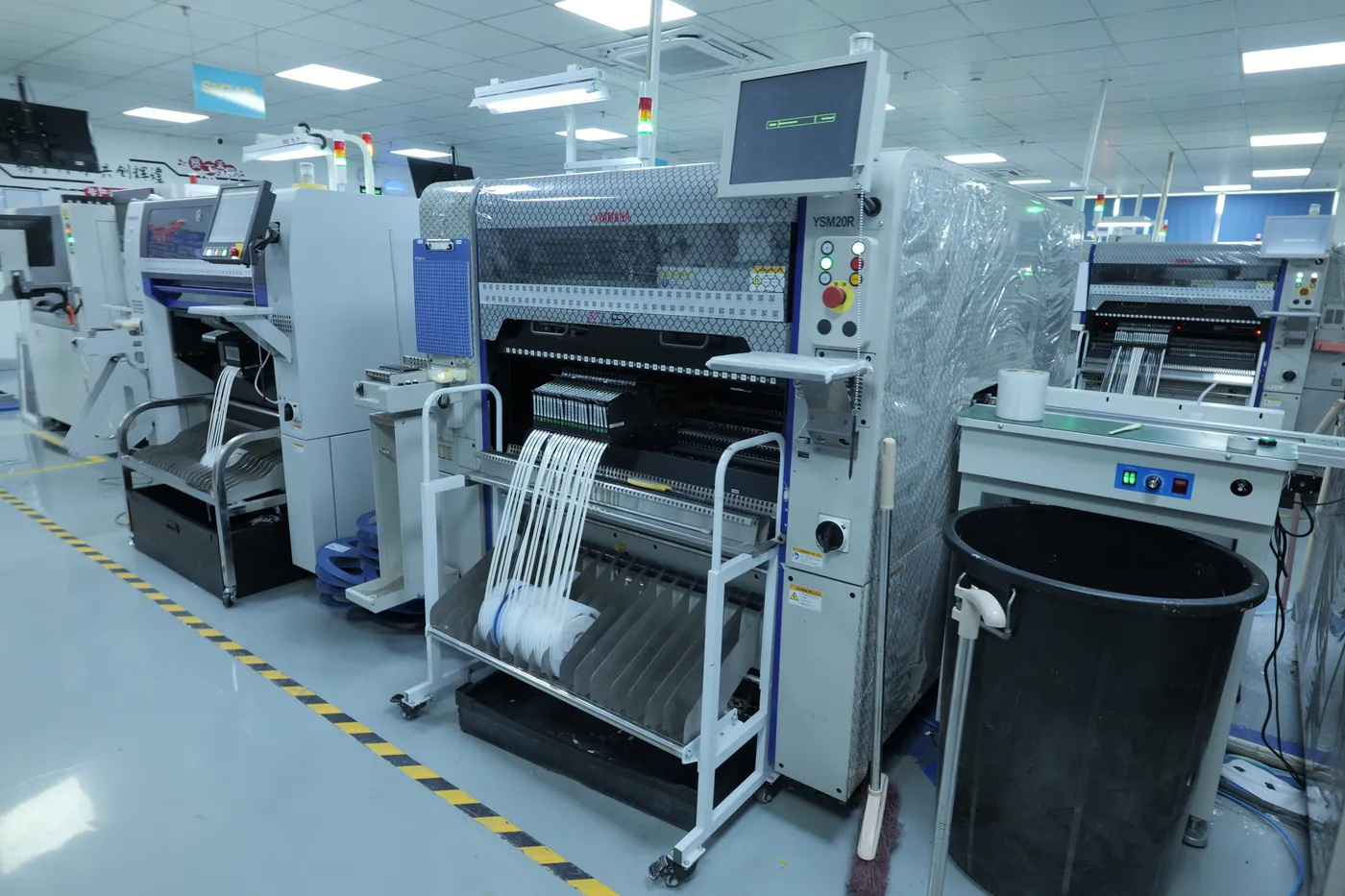
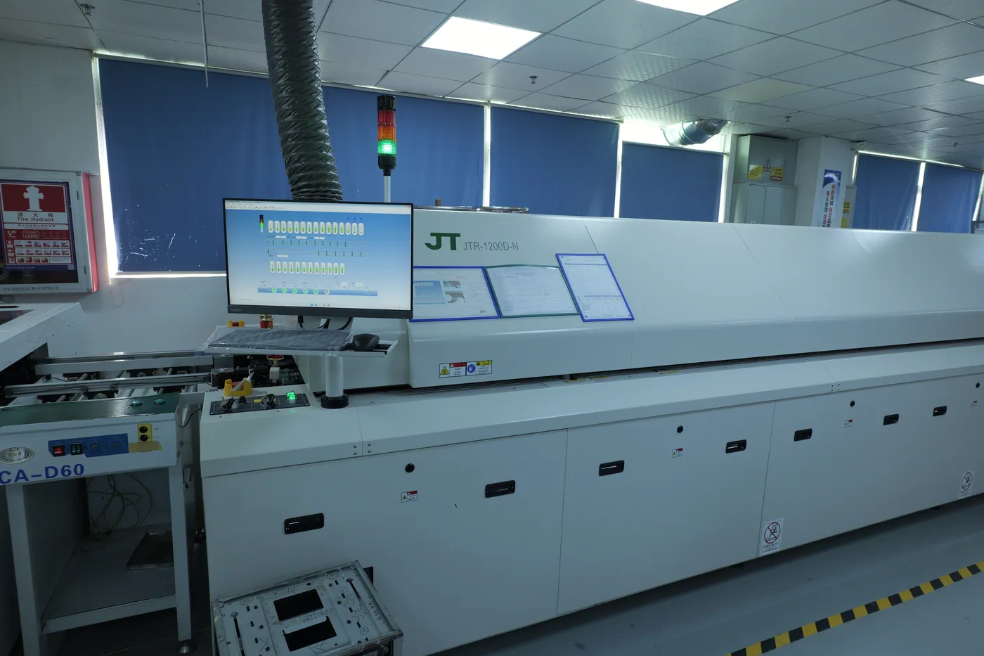
Solder Paste Printer
Zhengshi A5
7 LINES
3D SPI
SINIC-TEK
7 UNITS
SMT Pick & Place
Yamaha YSM10 + YSM20/20R
7 LINES
Reflow Oven
12-zone · J-STD-020
4 UNITS
Wave / DIP
Wave + selective
2 + 2
Inline Inspection
3D SPI · AOI · X-Ray
INLINE
IPC-A-610 Cl 2/3
The acceptance standard for every solder joint on every board.
FAI
First-article inspection and 4-party sign-off before batch runs.
IPQC
In-process checks at every stage — drift is caught on the line.
OQC
Final audit on every batch before it is packed and shipped.
Want the complete quality picture?
See how IPC-A-610 Class 2/3, FAI, IPQC and OQC connect into one documented quality system — from incoming inspection to final audit, with traceability on every batch.
common questions
Questions Procurement Teams Ask
What board sizes and layer counts can you build?
PCB fabrication: up to 32 layers, 2.5/2.5 mil HDI, panels up to 600 × 1200 mm. SMT assembly: boards 50×50 – 810×460 mm, 0.3–6.5 mm thick, from 03015 chips to 0.35 mm-pitch BGA.
How fast is your quick-turn?
48 hours from board-ready to first article on standard prototype builds, with an on-time rate above 95%. Pilot and production runs are scheduled per line loading.
What is your minimum order quantity?
EVT prototypes from 10–50 pcs and DVT pilots from 50–200 pcs; production MOQ depends on build complexity. Send your BOM and Gerber files for a same-day quotation.
Can we visit or audit the factory?
Yes — book a live video walk-through of the lines, or send your quality team for an on-site audit. Both start under NDA.
What quality systems does the facility run on?
JUZHITECH holds ISO 9001, ISO 13485 and IATF 16949 quality systems; production is built to IPC-A-610 Class 2/3 with RoHS/REACH compliance.
Trusted & Certified
Quality systems held by JUZHITECH — trusted by 500+ project teams worldwide for turnkey PCBA