Opens in a new tab
How We Design PCB

Custom PCB Design & Engineering Services

JUZHITECH provides board-level hardware design, high-speed PCB layout, embedded firmware, and DFM/DFT support to turn your requirements into production-ready PCBAs. From JDM and ODM development to pre-production reviews for OEM / EMS projects, our engineering team designs with manufacturing in mind.

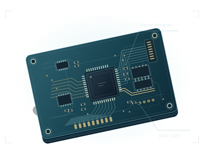
Engineering design view

3D PCB engineering view showing board outline, components, and copper layers for design verification
Designed for the way it will be built.
  • 6
  • Design Disciplines
  • 20+ yrs
  • PCB Engineering Experience
  • DFM / DFT
  • Design for Manufacturing & Testability

Six Design Disciplines

Full-stack PCB design.

Every discipline operates standalone or integrates into a complete turnkey PCB design workflow.

Schematic Capture & Hardware Architecture

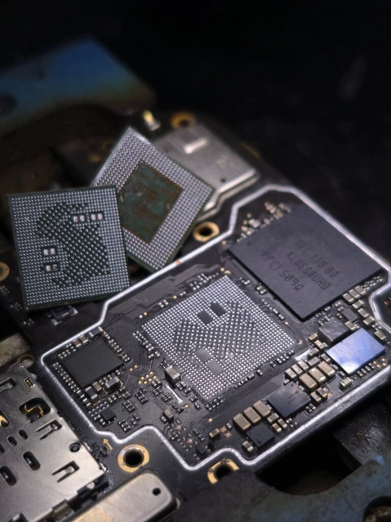
SoC selection, system architecture, and schematic capture. We build the engineering foundation using MCU vs MPU decision frameworks, power tree design, and precise peripheral mapping. Phase 1 of the PCB engineering workflow.

SoC SelectionSchematic CaptureBlock DiagramPhase 1
Explore Schematic & Architecture →
Soc select

PCB Layout & High-Speed Design

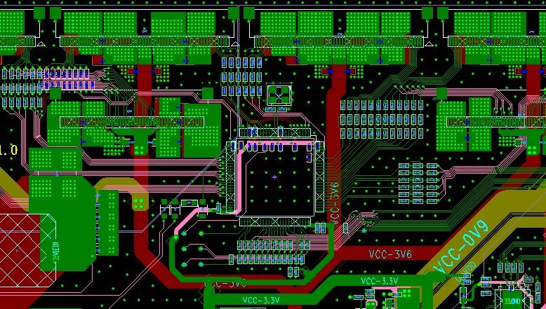
HDI stackup design, DDR/PCIe/USB routing with controlled impedance, precise length matching, and crosstalk mitigation. We engineer layouts from 4 to 32 layers with optimized PDN (Power Delivery Network) structures and strict DRC sign-off. Phase 2.

HDIFrom 4 to 32 layersDDR4 RoutingPhase 2
Explore PCB Layout →
PCB layout design: CAD view of printed circuit board component placement, copper traces, and routing

Embedded Firmware & Software Development

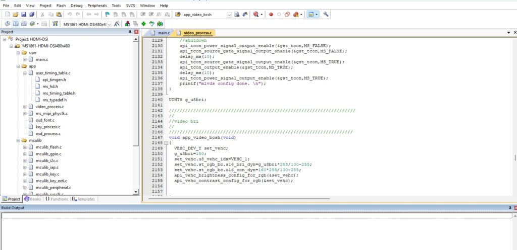
Bare-metal C, FreeRTOS, and Zephyr RTOS. We deliver BSP development, secure bootloader design, peripheral drivers, OTA update architecture, and production test firmware for your PCBA. Phase 3.

BSPFreeRTOSZephyrPhase 3
Explore Embedded Firmware →
Firmware development interface: embedded firmware code editor, build tools, and debugging console for custom hardware and PCBA platforms

DFM / DFT Review & NPI Support

Design-for-manufacturing review, test fixture design, and EVT→DVT→PVT transition management. We catch pad geometry and clearance issues before they become production delays. Phase 4.

DFMDFTNPIPhase 4
Explore DFM & NPI →
DFM and DFT review for PCB assembly, checking manufacturability and testability before mass production
Specialized Capabilities — woven into every stage of design

IoT & Wireless Hardware Design

BLE, LoRa, Wi-Fi, and Zigbee implementation. We execute RF PCB layout with impedance-matched antenna feeds, matching network design, low-power state strategies, and FCC/CE design-stage EMC review with partner-lab pre-compliance.

BLELoRaRF LayoutSpecialized
Explore IoT Hardware →
IoT wireless gateway board: custom PCBA with wireless connectivity for IoT device networking and edge data transmission

BOM Optimization & Component Engineering

Alternative component validation, lifecycle EOL tracking, multi-source strategies, and IC shortage mitigation. We cross-reference your BOM against authorized distributor stock to reduce costs without reliability compromise.

BOM Cost-DownEOL RiskAlternate PartsSpecialized
Explore BOM Optimization →
BOM optimization and component engineering for PCBA manufacturing: reviewing the bill of materials, component selection, and cost reduction
Mutual NDA
ISO 9001 · ISO 13485 · IATF 16949
IPC-A-610 Class 2 / Class 3
Direct Engineer Access

How We Design

Four phases — from concept to production-ready PCB.

Every PCB design project follows this structured engineering sequence.

01

Architecture & Component Selection

SoC evaluation, block diagram, power tree, and target BOM cost locked before schematic capture.

02

Schematic & PCB Layout

Schematic capture, HDI stackup, controlled-impedance routing, delay tuning, PDN layout optimization, and rigid DRC sign-off.

03

Prototyping & Firmware

Quick-turn PCBA fabrication, BSP bring-up, firmware development, and EVT/DVT validation cycles.

04

DFM Review & NPI Sign-Off

Manufacturability review, test strategy mapping, PVT ramp, and production handoff documentation.

Our Approach

Integrated PCB design and manufacturing — engineering continuity produces better PCBA.

PCB design and SMT assembly under one roof

Separating PCB design from PCBA manufacturing creates an information gap—the primary cause of prototype failures and production delays. JUZHITECH eliminates this risk. As an engineering-led turnkey PCBA manufacturer, the hardware engineers who design your board sit steps away from the SMT lines that build it, all operating under our ISO 9001/13485/16949 quality system.

This integrated approach to custom PCB design and assembly produces three structural advantages. First, design for manufacturability (DFM) is a live conversation, not a post-handoff report — our process engineer reviews your layout before Gerber release and flags pad geometry, solder mask clearance, and via-in-pad issues while they cost nothing to fix. Second, component selection and BOM optimization happen during schematic design — every part is verified against authorized distributor stock and lifecycle status before layout begins, so your PCBA design for manufacturing starts with a buildable BOM, not a wish list. Third, test strategy is developed alongside the PCB layout — ICT test points, boundary scan access, and FCT fixture interfaces are designed in from day one, not retrofitted after the first prototype reveals they're missing.

What this means for your project:

fewer prototype iterations, higher first-pass PCBA manufacturing yield, and a single point of accountability for your entire electronic product design and development — from concept to shipped boards.

End-to-end PCB design services — six coordinated disciplines.

Production-ready turnkey PCBA design requires more than schematic capture and PCB layout — it requires six engineering disciplines working in lockstep. At JUZHITECH, they work under one roof, steps away from the SMT lines that will build your board.

  • Hardware system architecture — SoC/MPU selection with cost-performance trade-off analysis, peripheral mapping, power tree design, and clock distribution planning. These decisions determine BOM cost, layer count, firmware complexity, and supply chain resilience.
  • High-speed PCB layout and HDI design — Controlled impedance routing for DDR, PCIe, and USB. HDI stackups with blind, buried, and micro vias. Delay tuning, phase matching, and crosstalk mitigation — signal integrity engineered in, not guessed at.
  • Embedded firmware development — Bare-metal C, FreeRTOS, or Zephyr. BSP with low-level drivers, secure bootloader, and production test firmware.
  • IoT and wireless hardware design — BLE, LoRa, Wi-Fi, Zigbee. RF PCB layout with impedance-controlled antenna feeds, matching network design, and FCC/CE design-stage EMC review with partner-lab pre-compliance.
  • BOM optimization and component engineering — Alternative component validation, lifecycle EOL tracking, and multi-source strategies against authorized distributor stock.
  • DFM review, DFT strategy, and NPI transition — Manufacturability and test reviews executed by the process engineers who run our SMT lines. EVT → DVT → PVT → MP.

Design in Practice

From 4-layer prototype to production-grade HDI PCBA — in one engagement.

A smart home OEM engaged us through a JDM (Joint Design) collaboration in Q3 2025. Their existing 4-layer prototype failed CE radiated emissions and carried a per-unit BOM cost above target. Our team re-architected the PCB as a 6-layer HDI stackup — reducing board area by 35%, passing radiated emissions at the accredited lab on the first submission, and cutting per-unit BOM cost by 18% through standardized passives and alternate MCU sourcing.

4→6HDI Layers
−35%Board Area
−18%BOM Cost
IoT wireless gateway board: custom PCBA with wireless connectivity for IoT device networking and edge data transmissionSMART HOME · HDI · CE

Technical Scope

PCB design & engineering capabilities at a glance.

Design DomainTechnologies & CapabilitiesStandards
PCB Layers1–32 layers, HDI with blind/buried/micro vias, via-in-pad, rigid and rigid-flexIPC-6012 Class 2/3
High-Speed InterfacesDDR3/DDR4/LPDDR4, PCIe Gen 3/4, USB 3.x, MIPI DSI/CSI, HDMI, 1G/10G EthernetJEDEC, PCI-SIG
Impedance Control50Ω single-ended, 100Ω/90Ω differential — ±10% standard, ±5% precision with TDR verificationIPC-2141
High-Speed ConstraintsPrecise length/delay tuning, phase matching, crosstalk mitigation, and PDN copper pouring rulesIPC-2221 / IPC-2222
RF & WirelessImpedance-matched antenna feeds, microstrip/stripline/CPW, via stitching, shieldingFCC Part 15, CE RED
Embedded FirmwareBare-metal C, FreeRTOS, Zephyr — BSP, bootloader, OTA, production test firmwareMISRA C, IEC 62304
EDA PlatformsAltium Designer, KiCad, Cadence Allegro/OrCAD — native and Gerber/ODB++/IPC-2581 handoffRS-274X/X2, ODB++

Common Questions

PCB Design & Engineering — FAQs

We work natively in Altium Designer, KiCad, and Cadence Allegro/OrCAD. We also accept Gerber RS-274X/X2, ODB++, and IPC-2581. If you’re transitioning from a different EDA platform, we can convert your existing files during onboarding.

PCB design timelines vary by complexity — a single-MCU 4-layer board moves faster than a 12-layer HDI design with precise DDR4 routing constraints. During architecture, we provide a detailed milestone schedule. As reference, schematic-to-Gerber cycles range from 2–8 weeks. Every project gets a confirmed schedule — not an estimate — before engineering starts.

Yes — DFM review is built into every project, not sold separately. Our process engineers review your layout before Gerber release, catching pad geometry, solder mask clearance, and via-in-pad issues at design stage. For OEM/EMS builds, DFM review is a pre-production gate with a formal report.

Every engagement starts with a mutual NDA signed before the first technical discussion. Your schematics, Gerber files, BOM, firmware, and product specifications remain your exclusive IP — stored on access-controlled servers and never shared with third parties.

Yes. We translate your PRD or block diagram into detailed hardware architecture: SoC evaluation, peripheral selection, power tree, and full schematic capture. We begin with a feasibility assessment where a senior engineer validates what’s achievable at your target BOM cost.

Design NRE depends on layer count, high-speed content, wireless integration, and firmware scope. After the architecture phase we quote a fixed price with a milestone schedule — so you know the full cost before schematic capture begins, with no hourly billing surprises.

How we deliver this capability.

Our PCB design services are available across three engagement models — choose what fits your project.

Co-Develop Hardware

Joint Design (JDM)

Your software team + our hardware engineers — co-develop the board. BSP and firmware included.

Explore JDM →
Full Turnkey Product

Turnkey ODM

You define the requirements — we own the full design, prototyping, certification, and production.

Explore ODM →
Have Complete Design Files

Build-to-Print OEM / EMS

Your Gerber + BOM, our factory. DFM review, sourcing, SMT assembly — no design work needed.

Explore OEM / EMS →