DFM / DFT Review & NPI Support
A PCB layout can pass design rule checks and still cause problems in assembly or testing. JUZHITECH combines DFM/DFT reviews, test-access planning, and EVT/DVT/PVT support to help turn validated designs into production-ready PCBAs.
The Gap
Throwing Gerber files over the wall is the fastest way to kill your production schedule.
When a design-only firm finishes a PCB layout, they run a software DRC and send the Gerbers to a contract manufacturer. The CM's CAM engineer immediately finds fatal physical flaws: 0.4mm pitch BGAs with inadequate solder mask webbing, via-in-pad structures lacking epoxy fill specifications causing solder wicking, or tall connectors shadowing 0201 passives from the wave soldering wave.
These physical geometry conflicts force the CM to issue Engineering Queries (EQs). The layout team has to revise the board, generating a new Gerber package. This iteration loop delays your prototype by weeks and inflates your NRE costs before a single component is placed.
How We Close It
DFM executed by the process engineers who actually run the SMT lines.
At JUZHITECH, DFM is not a post-design afterthought — it is a pre-release gate. The exact same SMT process engineers who run our Yamaha placement lines review your layout before Gerber generation. They don't just check for shorts; they analyze solder paste stencil aspect ratios, thermal mass imbalances that cause tombstoning, and physical clearances for automated optical inspection (AOI) camera angles.
This creates a zero-friction NPI transition. Because the factory verified the layout during the design phase, your first EVT prototype is built on a process-proven foundation. We eliminate the Gerber revision loop entirely.
Three Reviews
DFM, DFA, and DFT
These are not synonyms. DFM checks the board. DFA checks the assembly process. DFT checks whether you can verify the result.
| Review | Focus | Checked By | Typical Catch |
|---|---|---|---|
| DFM | Bare board fabricability — trace/space, annular ring, copper balance, via aspect ratio, solder mask clearance, surface finish compatibility | PCB fabrication engineer | Trace width below etching tolerance on layer 3 after compensating for 1.2-mil undercut |
| DFA | Assembly process — component placement, stencil aperture, reflow profile compatibility, connector access, depaneling method | SMT process engineer | 0201 capacitor placed 6 mil from a tall inductor, creating a solder shadow during reflow |
| DFT | Testability — ICT test point coverage, boundary scan chain access, FCT fixture interface, programming header reachability | Test development engineer | Critical net has no test point because the only accessible via is covered by a heatsink in the assembled state |
DFM, DFA, and DFT reviews happen before Gerber release — not after the first prototype reveals the issue. Each review is executed by the engineer who owns that process on the production floor, because a checklist written by someone who has never run an SMT line catches the theoretical problems but misses the real ones.
Physical Constraints
Standard DRC misses factory realities. We catch them before fabrication.
Our DFM review targets the physical physics of reflow, wave soldering, and automated assembly. Here are six common layout failures we intercept daily.
Uncapped via-in-pad causing solder wicking.
Routing a via directly inside a BGA pad saves space, but if left open, capillary action during reflow sucks the solder paste down the barrel, starving the joint and causing intermittent open circuits. We mandate VIPPO (Via-in-Pad Plated Over) with epoxy fill and copper capping for all BGA breakouts under 0.65mm pitch.
Thermal mass imbalance causing tombstoning.
Connecting one pad of an 0402 passive directly to a massive copper ground plane while the other connects to a thin 10-mil trace creates uneven heat dissipation during reflow. The hotter pad melts first, pulling the component vertical. We enforce strict thermal relief spoke geometries to equalize thermal mass on all discrete passives.
Solder mask slivers on fine-pitch components.
On 0.4mm pitch ICs, the solder mask web between pads can become too thin (under 3 mil) for the fabricator to reliably print, resulting in mask lift-off and solder bridging between pins. We review your clearance rules against our fabricator's exact LDI (Laser Direct Imaging) tolerance limits.
Component shadowing and wave solder orientation.
Tall through-hole components placed immediately upstream of surface-mount passives block the flow of molten solder during wave soldering, creating dry joints. We verify the physical orientation of the board through the wave and enforce strict keep-out zones behind tall components.
Test points placed under connectors or mechanical components.
ICT test points placed directly beneath an RJ45 jack or a mounting bracket. The flying probe can't reach them in the assembled state, so those nets are untestable on the production line. Fix: define a test access side during layout — typically the bottom side — and keep all test points clear of assembled component shadows.
Panelization stress on edge connectors and BGAs.
V-score placed 40 mil from a USB-C edge connector. During depaneling, the mechanical stress fractures the connector's solder joints — passing ICT immediately after assembly, but failing after 50 insertion cycles in the field. Fix: maintain minimum 120-mil clearance from V-score and routed slots to any connector or BGA package.
Cost of Delay
A DFM issue found at layout costs nothing. The same issue found on the SMT line costs a production batch.
The cost of fixing a design problem grows exponentially with each stage it survives undetected. Here's the gradient — and why we catch issues before Gerber generation.
| Stage Found | Fix Cost | Schedule Impact | What Happens |
|---|---|---|---|
| Layout phase (in-house) | $0 | Zero delay | Layout engineer fixes it in the native CAD file. No one outside the team knows it existed. |
| Gerber review (pre-release) | Low — engineering time only | +1–2 days | Re-open CAD, modify, re-export Gerber, re-run DFM check. Minimal cost, minor schedule slip. |
| Post-Gerber / pre-production | Medium — re-spin NRE | +3–5 days | Fabricator CAM engineer flags the issue. Gerber revision required. CAM re-processing fee applies. Panelization re-done. |
| On the SMT line (post-assembly) | High — rework + scrap + re-spin | +1–3 weeks | Batch fails ICT or FCT. Root cause analysis determines layout origin. Partial or full batch scrapped. Redesign, re-fab, re-assembly. Customer delivery delayed. |
| In the field (customer return) | Catastrophic — recall + re-spin + brand damage | +4–12 weeks | Field failures trigger RMA investigation. Root cause traces to a DFM issue that survived every gate. Recall cost, rework cost, contract penalty, and a customer who sources elsewhere next time. |
A 2-hour review session between a layout engineer and a process engineer costs roughly the same as one re-spin's CAM processing fee — and catches the issues that would otherwise become that re-spin. The math is not complicated.
Design for Test
Design for Test (DFT) — because you cannot ship what you cannot verify.
Production speed is dictated by test time. If your board requires an operator to manually probe pins with a multimeter, your throughput collapses. We design testability into the layout.
ICT (In-Circuit Test) — mapping the bed of nails.
ICT verifies the physical assembly: correct component placement, values, polarity, and the absence of open/short circuits. To achieve high test coverage, the layout must provide physical access for the test fixture's pogo pins. Our engineers mandate dedicated test points (typically 0.8mm to 1.0mm diameter) on every critical net. We enforce a minimum 50 mil clearance from test points to component bodies to prevent pogo-pin mechanical interference.
FCT (Functional Test) — fixture design and automation.
FCT proves the board actually works. Instead of manual testing, we design custom mechanical FCT fixtures with automated pneumatic or toggle-clamp engagement. The fixture powers the board, flashes the production firmware via JTAG/SWD, and executes a fully automated test script communicating over UART or CAN. We verify ADC tolerances, radio RSSI levels, and GPIO states in seconds, writing the telemetry directly to the factory database.
Boundary scan (JTAG) coverage is verified during the DFT stage — we validate the IEEE 1149.1 chain integrity for all BGA and fine-pitch devices before fixture design, ensuring nets inaccessible to physical probes are still testable.
Strain-gauge testing for press-fit components.
For industrial and telecom boards utilizing press-fit connectors, improper insertion force damages the inner plating of the PCB vias. During the NPI transition, we perform strain-gauge testing to map the mechanical stress applied to the board during connector insertion and fixture clamping, ensuring the physical force remains strictly within IPC guidelines.
In Practice
DFM in Practice
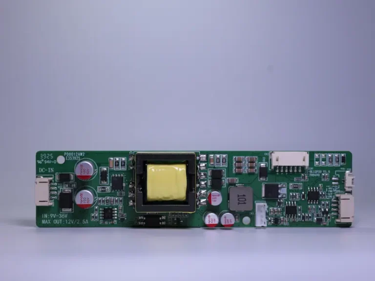 INDUSTRIAL · PCIe GEN 4 · 8-LAYER
Industrial Automation PCBA
11 DFM issues in a DRC-clean 8-layer PCIe Gen 4 carrier board — caught before Gerber release.
An industrial automation client submitted an 8-layer PCIe Gen 4 carrier board for DFM review. The layout had passed DRC in Altium with zero violations. The client's original fabricator had already quoted the board, and the schedule was locked for a 200-unit prototype batch.
Our process engineer found 11 DFM issues in a single review session: solder mask slivers between 0.4mm-pitch BGA pads that would bridge during reflow, via-in-pad without copper fill on a QFN thermal pad that would wick solder away from the joint, acute-angle trace entries creating acid traps on three BGA fanouts, and test points placed directly under a heatsink footprint — making those nets completely untestable at ICT.
Every issue was fixed in the native CAD file before Gerber export — zero cost, zero schedule impact. The same issues caught after SMT would have scrapped a 200-unit prototype batch: $8,500 in re-fabrication cost and a 3-week schedule slip.
NPI Framework
The EVT to Mass Production transition
Scaling from 10 prototypes to 10,000 units requires strict version control, yield analytics, and process locking. We manage the entire NPI lifecycle.
10 – 50 units
- Bare-board hardware bring-up
- Clock tree & power sequence scoping
- Initial DFM feedback integration
- Critical bug isolation (Code vs. Copper)
50 – 200 units
- Form, fit, and function lock
- EMC design-stage review & pre-compliance coordination (partner lab)
- Thermal & environmental stress testing
- Yield baseline establishment
200 – 500 units
- SMT & DIP SOP (Standard Operating Procedure) locked
- FCT (Functional Test) fixture automation
- Solder paste stencil & profile optimization
- Packaging and pack-out sequence verified
1,000+ units
- Continuous yield monitoring & analytics
- Shift-to-shift consistency control
- Alternative component (second source) rollout
- Sustained lifecycle management
Common Questions
DFM / DFT review & NPI FAQ.
What's the difference between DFM and DFT ?
DFM (Design for Manufacturing) ensures the bare PCB can be fabricated reliably and components can be soldered without defects (e.g., checking pad geometries, solder mask clearances, and thermal reliefs). DFT (Design for Test) ensures the assembled board can be efficiently verified on the production line (e.g., placing accessible test points for pogo-pins, adding JTAG headers, and routing debug UARTs). We perform both simultaneously before Gerber release.
When should DFM review happen ?
DFM must happen before layout freeze, not after. If you wait until the Gerbers are generated to ask a manufacturer for DFM feedback, fixing the issues requires reopening the CAD file, adjusting the layout, re-tuning high-speed delays, and generating new files. We integrate DFM checks continuously during the layout phase to eliminate this revision loop.
What's involved in the EVT → DVT → PVT transition ?
EVT (Engineering Validation Test) validates that the design works — 10 to 50 hand-assembled units, functional testing, initial DFM feedback. DVT (Design Validation Test) validates the production-intent design — 50 to 200 units built with production tooling, real enclosures, production BOM with alternate components,EMC design-stage review with partner-lab pre-compliance coordination. PVT (Production Validation Test) validates the production process — 200 to 500 units built on the production line at production speed, process capability study (Cpk ≥ 1.33), operator training, yield target verification. Each stage gates the next: a design that can’t hit 95% first-pass yield at PVT does not proceed to mass production.
Do you build custom FCT (Functional Test) fixtures in-house ?
Yes. We design and CNC-machine custom test enclosures (clamshell or pneumatic) tailored to your PCBA’s exact dimensions. We populate them with the correct pogo-pin arrays, wire them to automated test instruments, and write the Python or LabVIEW test scripts that execute your functional validation sequence on the factory line.
Do you provide DFM review as a standalone service ?
Yes — if you have a completed PCB layout and need a manufacturability review before sending it to fabrication, we provide a standalone DFM/DFA/DFT review with a formal report. The review is executed by the same process engineers who run our production lines — not a junior engineer reading an IPC checklist. We deliver a prioritized issue list with recommended fixes, Gerber markups, and a go/no-go recommendation for fabrication. For clients who then proceed to manufacturing with us, the review fee is credited toward the production order.
How We Deliver
Our process engineering bandwidth is available through three engagement models — from design review to full production transition.
Joint Design (JDM)
We co-develop the hardware with your team, embedding DFM rules from schematic day one and managing the entire NPI ramp in our factory.
Explore JDM →Full Turnkey ProductTurnkey ODM
We own the full design, DFM review, test strategy, NPI transition, and production lifecycle under one roof and one quality system.
Explore ODM →Have Complete Design Files?Build-to-Print EMS
You provide the locked Gerber and BOM. We execute a rigid DFM pre-check, issue a formal report, and transition your files to mass production.
Explore OEM / EMS →