Schematic Capture &
Board-Level Hardware Design
From MCU/MPU selection and power architecture to precision schematic capture, we build the electrical foundation of your PCBA. Our engineering approach considers performance, BOM cost, PCB layout constraints, and firmware integration before routing begins.
The Gap
Most PCBA projects start with a component choice — and that single decision cascades into cost, performance, and availability for the product's entire lifecycle.
Choose the wrong SoC and your firmware team spends months patching a broken BSP. Over-spec the power tree and you're locked into a higher BOM cost at every production run. Miss a signal chain detail and your first prototype fails EMC. These aren't assembly problems — they're architecture problems, and they're the most expensive to fix because the fix propagates backward through schematic, layout, and firmware.
How We Close It
A structured hardware architecture process — defining physical constraints before routing traces.
We translate your product requirements into a detailed system architecture through four phases: feasibility assessment, SoC selection with cost-vs-performance trade-off analysis, power tree and clock distribution design, and full schematic capture with DRC validation. Every decision is documented, every trade-off is presented for your review, and every schematic leaves our team DFM-reviewed by the same process engineers who will build your boards — not a remote reviewer who has never seen an SMT line.
Decision Framework
SoC selection — Mitigating BOM cost and EOL risk.
The processor you choose dictates your BOM cost, PCB layer count, firmware effort, and supply chain resilience. This matrix covers the architecture families our engineering team implements daily.
| Architecture | Max Clock | Typical RAM | OS Support | Typical Layers | BOM Cost Level | Best For |
|---|---|---|---|---|---|---|
| Cortex-M0/M0+ | 48 MHz | 8–64 KB | Bare-metal / RTOS | 2–4 | $ | Simple sensor nodes, battery-powered IoT endpoints, basic control |
| Cortex-M3/M4 | 72–180 MHz | 64–512 KB | FreeRTOS / Zephyr | 4 | $$ | Motor control, consumer IoT, industrial sensing with DSP |
| Cortex-M7 | 300–600 MHz | 512 KB–2 MB | FreeRTOS / Zephyr | 4–6 | $$ | Real-time audio, high-speed control loops, edge AI inference |
| Cortex-A (A7/A53/A55) | 1.0–2.0 GHz | 256 MB–2 GB (DDR) | Embedded Linux | 6–10 | $$$ | HMI products, AI edge gateways, multi-protocol IoT hubs |
| RISC-V (MCU class) | 100–400 MHz | 64–512 KB | FreeRTOS / Zephyr | 4 | $–$$ | Supply chain diversification, cost-sensitive IoT, open-ISA projects |
| FPGA + SoC hybrid | Varies | DDR on-chip | Linux + Bare-metal | 8–14 | $$$$ | High-speed data acquisition, software-defined radio, vision processing |
This is a decision framework, not a datasheet. Final selection depends on exact I/O mapping, power budgets, and target unit cost at volume. We present options with delta reports; you make the final call.
Design Domains
Domains of custom circuit design
A production-ready PCBA schematic rarely lives in a single design domain. A wireless IoT gateway combines analog sensor front-ends, high-speed digital buses, multi-rail sequencing, and RF matching—all on one schematic, delivered by one specialized engineering team.
Analog signal conditioning
Low-noise op-amp circuits with active filtering, precision ADC front-ends with anti-aliasing, and bridge sensor excitation with ratiometric referencing. Designed for measurement-grade PCBA.
Digital system integration
MCU/MPU memory bus architecture (QSPI, eMMC, DDR), precise peripheral mapping against pin-mux constraints, and level-translation between voltage domains.
Mixed-signal partitioning
ADC/DAC integration with isolated ground planes, single-point star grounding strategies, guard rings around high-impedance nodes, and digital-return-path isolation.
Power management & sequencing
LDO vs. DC-DC topology selection balancing efficiency and noise. Multi-rail power sequencing with enable-chaining, PG-good monitoring, and battery fuel gauging.
High-speed digital interfaces
DDR3/DDR4 routing constraints with fly-by topology and VTT termination rules defined at the schematic level. PCIe Gen 3/4 lane allocation, USB 3.x SuperSpeed, and RGMII/SGMII Ethernet PHY integration.
Sensor & actuator interfaces
Thermocouple cold-junction compensation, MEMS IMU integration, capacitive touch sensing with active shields, and 4–20 mA industrial current-loop receivers.
Methodology
How we lock board-level hardware architecture for PCBA.
Requirements analysis — translating product goals into engineering constraints.
Hardware architecture begins with your product requirements — not a datasheet. Our team works from your PRD, target BOM cost, and volume projections to define the engineering constraints that drive every downstream decision: maximum power envelope, I/O count and type, mechanical form factor limits, regulatory requirements (FCC, CE, medical, automotive), and target unit cost at volume. If certain constraints conflict — a BOM cost target that can't support the required processing performance — we flag the tension immediately and present trade-off options before a single component is selected.
SoC and component selection — a structured decision, not a preference.
Selecting the right IC is a multi-dimensional optimization problem. For every major component, we evaluate a shortlist against a strict matrix: technical fit, stock availability (via direct distributor API checks), lifecycle EOL status, second-source pin compatibility, and ecosystem maturity. You receive 2–3 options per critical component alongside a cost-benefit delta report.
A Cortex-M4 with internal LDO and on-chip flash needs a 4-layer board and a handful of decoupling caps. A Cortex-A55 with external DDR4, eMMC, and MIPI display needs 8–10 layers with controlled impedance, multiple power rails, and careful PDN design. The processor choice cascades into BOM count, layout complexity, firmware effort, and per-unit cost — which is why we lock it during architecture, not during schematic.
Schematic capture — discipline, not creativity.
Schematic design is an engineering discipline. We follow a structured methodology: modular hierarchical sheets organized by functional block (power, processor, memory, I/O, RF), consistent net naming conventions, DRC at every review gate, and component library management with verified IPC-7351 footprints. Every schematic is reviewed against our internal checklist: power sequencing, decoupling strategy, pull-up/pull-down defaults for every GPIO, reset circuit behavior during brown-out, and test point placement for ICT and FCT access. The output is a complete schematic package — hierarchical PDF, native source files, validated BOM with manufacturer part numbers and distributor links, and a design review report documenting every decision.
Design review gates — you approve before we proceed.
No schematic proceeds to PCB layout without your sign-off. We schedule formal reviews at each gate: requirements sign-off (architecture document + preliminary BOM cost), schematic review (complete schematic + validated BOM + component lifecycle report), and pre-layout review (schematic-to-footprint mapping + DFM pre-check). This gated process ensures your engineering, procurement, and firmware teams are aligned on the hardware architecture before a single trace is routed — catching the expensive mistakes that happen when schematic capture runs ahead of stakeholder review.
In Practice
From PRD to validated schematic — a dual-radio smart home controller.
How component selection and architecture decisions shaped a dual-radio BLE + Wi-Fi gateway.
Smart Home Gateway PCBA
Selecting a dual-radio SoC architecture for BLE + Wi-Fi coexistence
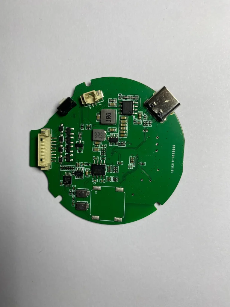
The client’s requirements specified simultaneous BLE mesh and 2.4 GHz Wi-Fi operation—a known RF coexistence challenge. We evaluated three SoC families against RF isolation metrics and BOM targets. We architected a dual-core solution (dedicating one core to the BLE stack and one to Wi-Fi) coupled with external RF front-end filtering. This topology achieved 35 dB of adjacent channel rejection at the hardware level, supporting FCC compliance without expensive metal shielding.
 Case study
Common Questions
Hardware architecture & schematic design FAQ
How do you choose between an MCU and an MPU for my product ?
The decision hinges on software requirements, target BOM cost, and PCB layer budget. If your firmware uses an RTOS with moderate I/O, a Cortex-M4 keeps the BOM low and fits on 4 layers. If you require embedded Linux, complex display frameworks, or heavy networking, a Cortex-A MPU is necessary—but it forces DDR routing, complex PDN design, and 6–10 PCB layers. We present these exact trade-offs during the feasibility stage.
What deliverables do I get from a schematic design engagement ?
You receive a complete production-ready package: hierarchical PDFs for review, native EDA source files (Altium or KiCad), a scrubbed BOM with manufacturer part numbers, and a lifecycle risk report. Every package also includes a pre-layout DFM checklist to ensure your subsequent PCB layout phase starts with manufacturable data.
Can you work from an existing schematic that needs review or optimization ?
Yes — schematic review and optimization is a common starting point. We audit your existing design against IPC standards, component lifecycle status, DFM requirements, and your target BOM cost. Typical findings: over-specified components that can be replaced with lower-cost equivalents, EOL parts requiring an alternate, missing decoupling or ESD protection, and power sequencing issues that would manifest at prototype. You receive a structured review report with prioritized recommendations.
Do you provide component sourcing recommendations during schematic design ?
Yes. Component availability is not an afterthought; it drives architecture. During schematic capture, every critical component is cross-referenced against authorized distributor stock (Mouser, DigiKey) and manufacturer lifecycle databases. We immediately flag parts with 12+ week lead times or EOL warnings. The BOM you approve at schematic sign-off is instantly buildable.
What if I only need schematic design — no PCB layout or firmware ?
Schematic design is available as a standalone engagement — you receive the complete schematic package and can hand it to your in-house layout team or another partner. We provide the schematic in your preferred EDA format with full documentation. If you later decide you want us to handle layout or manufacturing, the schematic is already on our platform and ready to proceed.
How We Deliver
Electronic hardware design available through two engagement models — from co-development to full turnkey.
Joint Design(JDM)
Your software team + our hardware engineers — co-architect the PCBA. SoC selection and schematic capture with your input at every gate.
Explore JDM →Turnkey ODM
You define requirements — we own the full hardware architecture, component selection, and production lifecycle.
Explore Turnkey ODM →Already have a complete schematic and BOM? Send your design files for manufacturing — DFM review, sourcing, and SMT assembly without design work.