PCB design and SMT assembly under one roof
Separating PCB design from PCBA manufacturing creates an information gap—the primary cause of prototype failures and production delays. JUZHITECH eliminates this risk. As an engineering-led turnkey PCBA manufacturer, the hardware engineers who design your board sit steps away from the SMT lines that build it, all operating under our ISO 9001/13485/16949 quality system.
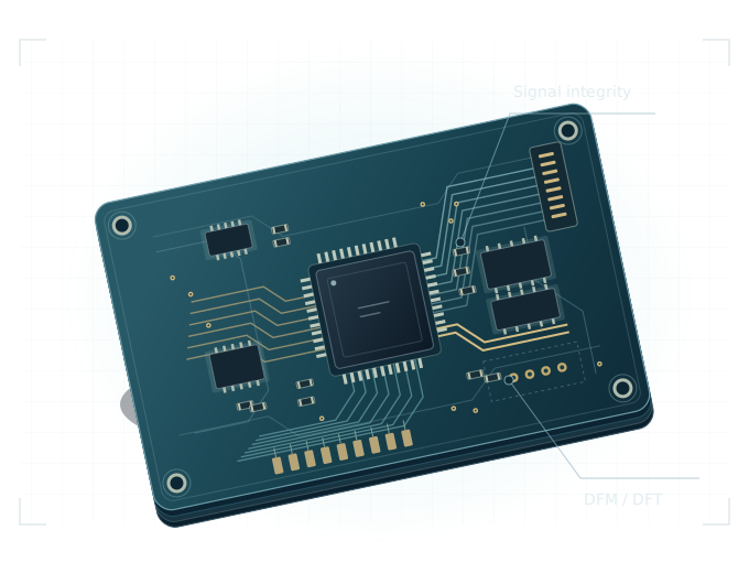
This integrated approach to custom PCB design and assembly produces three structural advantages. First, design for manufacturability (DFM) is a live conversation, not a post-handoff report — our process engineer reviews your layout before Gerber release and flags pad geometry, solder mask clearance, and via-in-pad issues while they cost nothing to fix. Second, component selection and BOM optimization happen during schematic design — every part is verified against authorized distributor stock and lifecycle status before layout begins, so your PCBA design for manufacturing starts with a buildable BOM, not a wish list. Third, test strategy is developed alongside the PCB layout — ICT test points, boundary scan access, and FCT fixture interfaces are designed in from day one, not retrofitted after the first prototype reveals they're missing.
fewer prototype iterations, higher first-pass PCBA manufacturing yield, and a single point of accountability for your entire electronic product design and development — from concept to shipped boards.
End-to-end PCB design services — six coordinated disciplines.
Production-ready turnkey PCBA design requires more than schematic capture and PCB layout — it requires six engineering disciplines working in lockstep. At JUZHITECH, they work under one roof, steps away from the SMT lines that will build your board.
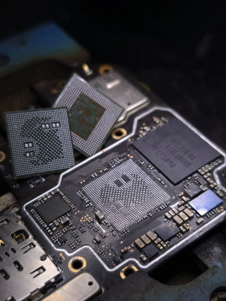
- Hardware system architecture — SoC/MPU selection with cost-performance trade-off analysis, peripheral mapping, power tree design, and clock distribution planning. These decisions determine BOM cost, layer count, firmware complexity, and supply chain resilience.
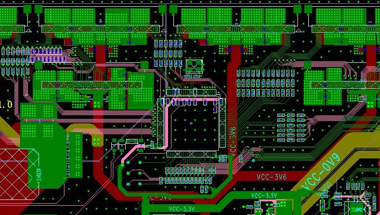
- High-speed PCB layout and HDI design — Controlled impedance routing for DDR, PCIe, and USB. HDI stackups with blind, buried, and micro vias. Delay tuning, phase matching, and crosstalk mitigation — signal integrity engineered in, not guessed at.
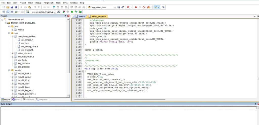
- Embedded firmware development — Bare-metal C, FreeRTOS, or Zephyr. BSP with low-level drivers, secure bootloader, and production test firmware.
- IoT and wireless hardware design — BLE, LoRa, Wi-Fi, Zigbee. RF PCB layout with impedance-controlled antenna feeds, matching network design, and FCC/CE design-stage EMC review with partner-lab pre-compliance.
- BOM optimization and component engineering — Alternative component validation, lifecycle EOL tracking, and multi-source strategies against authorized distributor stock.
- DFM review, DFT strategy, and NPI transition — Manufacturability and test reviews executed by the process engineers who run our SMT lines. EVT → DVT → PVT → MP.